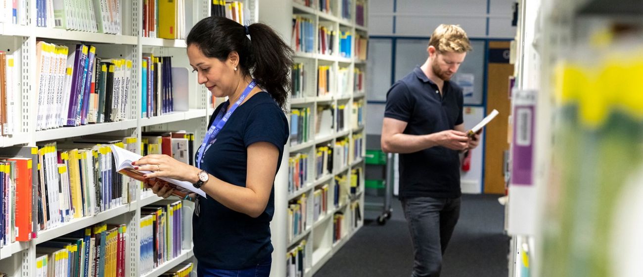
Research
With a focus on health, social justice and sustainability in an increasingly digital environment, our research has a positive impact on your world250+
research students currently enrolled at LSBU
95%
of our research is world-leading, internationally excellent or internationally recognised
£25m+
afforded to us in grants for research, delivering cultural benefits and improving lives
Research and Innovation Strategy 2030
At LSBU, our 2030 vision for research and innovation is to undertake distinctive research and innovation that benefits our local and global community. Find out more by downloading our strategy.
Research Centres
Working in tandem with our school-based university research groups, our research centres build on LSBU’s outstanding areas of institutional strength to support a greater concentration of interdisciplinary research and innovation.
A pivotal community of subject focussed research

Nicotine, Tobacco, and Vaping Research Group
This research group is dedicated to advancing psychological understanding of nicotine use and dependence and facilitating sustainable smoking cessation strategies. As tobacco smoking remains a significant contributor to preventable mortality, particularly among the most disadvantaged in society, our mission is to alleviate this burden of health inequality.

Centre for the Study of the Networked Image (CSNI)
CSNI aims to bring together researchers from cultural studies, software studies, contemporary art, media, and performance practice, who seek new knowledge and understanding of the myriad ways in which culture and society has been affected by computational systems.
Workforce INnovation Group (WING)
Effective healthcare workforce planning is vital to ensure appropriate levels and skills of staff are available to deliver safe, high-quality care to patients and service users.
WING's research has developed a detailed understanding of work that enables the building of models around the impact of staffing levels on patient outcomes; workload activity in complex areas; and contribution that specialist roles make.
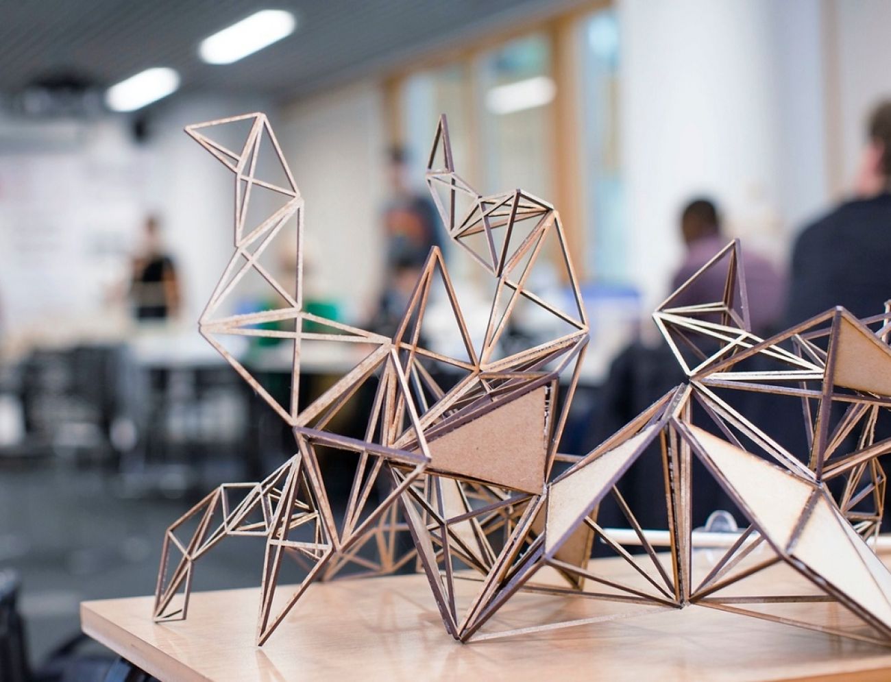
Mechanical Intelligence (MI) Research Group
By integrating knowledge from multiple disciplines, this research group explores the mechanical characteristics of nature, from the micro to macro scales, to innovate and enhance engineering systems.
Research covers everything from fundamental discoveries to real-world applications, paving the way for cutting-edge solutions in structural engineering, robotics, materials science, and beyond.

Smart Internet Technologies Hub (SITHub)
Smart Internet Technologies Hub (SITHub) specialises in the research and development of next-generation networking and cloud technologies, including Beyond 5G and 6G, programmable networks, edge-AI and AI/ML integration technologies. Their work covers edge to cloud continuum, integrated TN/NTN technologies, network automation, orchestration, and analytics.
Research & Innovation Portal
Explore the collaborative research and innovation work of our academic community and from colleagues across LSBU.
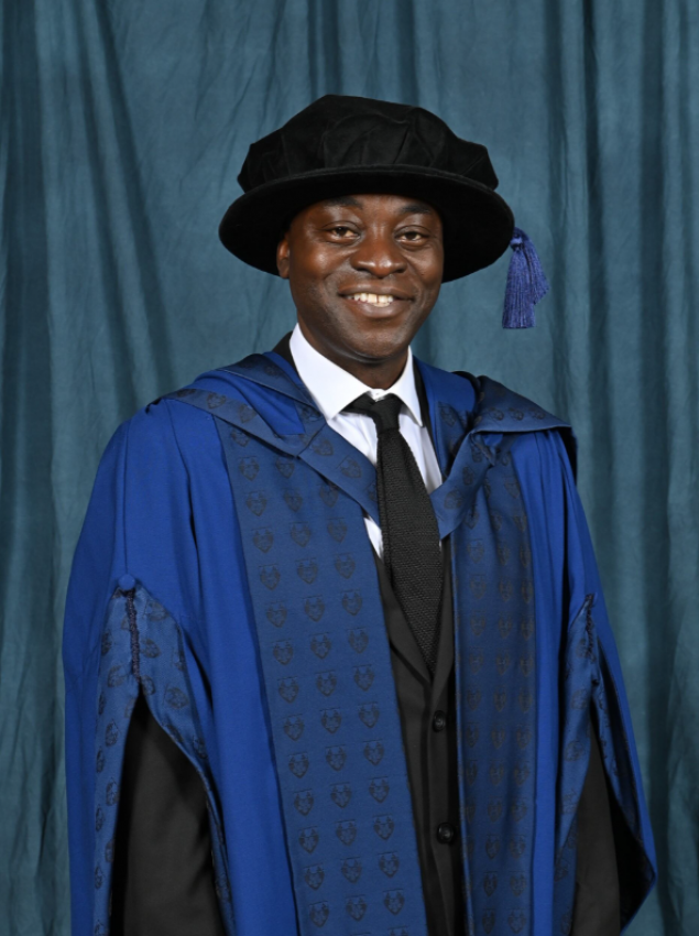
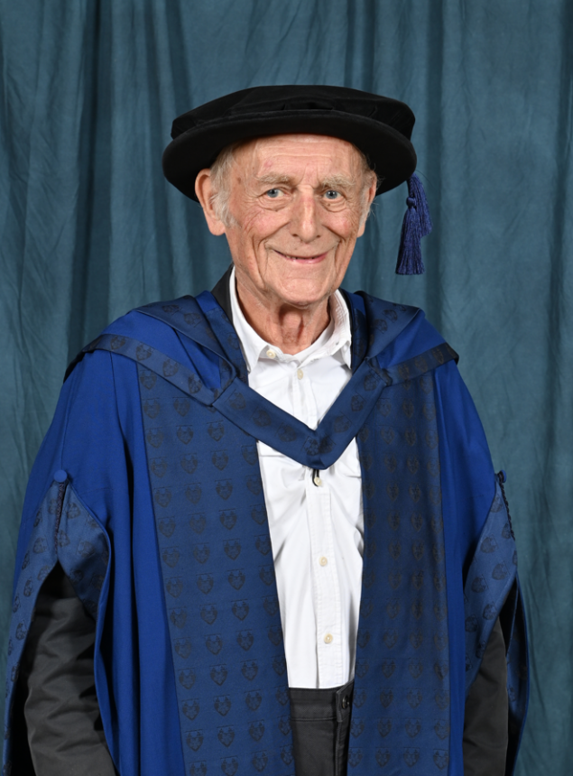
Charlie Dark MBE, Honorary Doctor of the Univ…
Stephen Addison BEM, honorary doctor of lette…
Stephen Addison has been made an honorary doctor of letters.

Honorary Doctor David Oyelowo OBE on the figh…
David Oyelowo OBE is one of this year’s Honorary Doctors in LSBU's School of the Arts and Creative Industries.
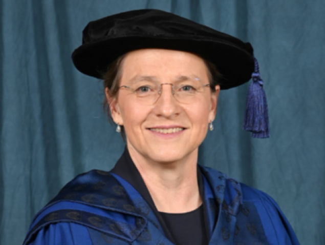
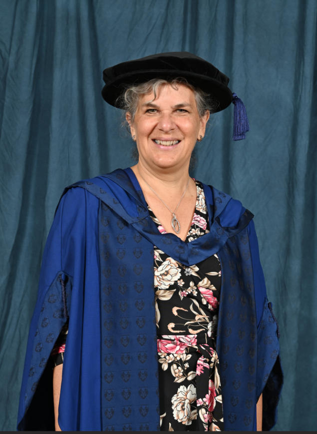
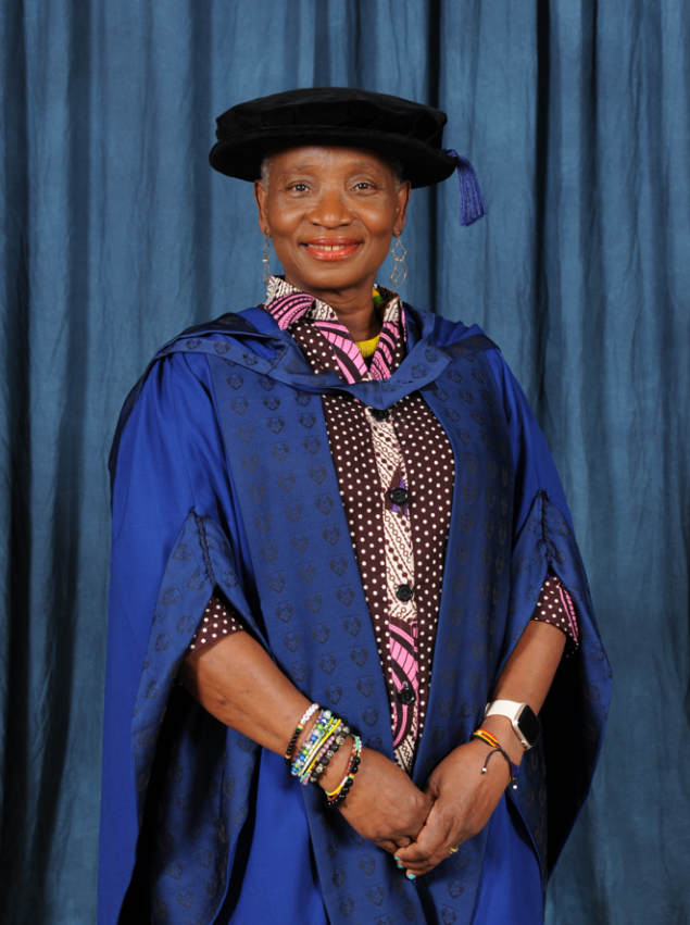
Sara Autton, Honorary Doctor of the Universit…
PhD student Carolyn Defrin on collaborating w…
Student and freelance artist, Carolyn Defrin, tells us about her collaborative research with Hammersmith United Charities and gives crucial advice to ...
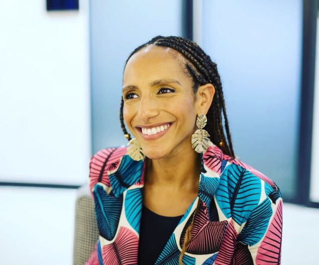
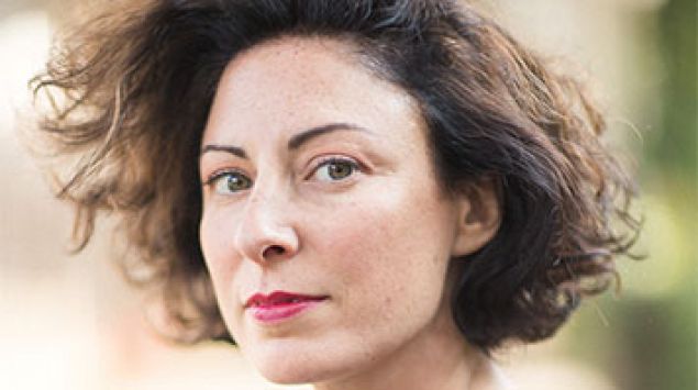
Afua Hirsch strikes out on her own
Afua Hirsch receives an honorary doctorate of letters.

London-based designer Lozana Rossenova undert…
Designer and PhD student, Lozana Rossenova, discusses her research in collaboration with not-for-profit arts organisation, Rhizome, which focuses on t...
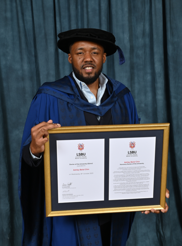
Ashley Belal Chin, Honorary Doctor of the Uni…
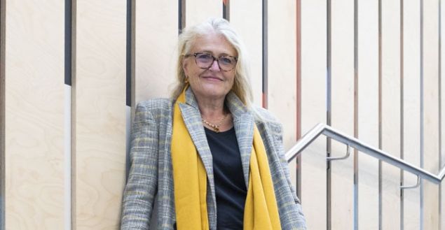
Miriam Rodway, Honorary Doctor of the Univers…

Zeta Kolokythopoulou on studying a PhD whilst…
Recent PhD graduate and Journal Development Specialist at Frontiers, Zeta Kolokythopoulou, discusses the obstacles she had to overcome to complete her...

Acoustics research helps improve safety and q…
Collaborative Urban Engineering applied acoustics research project with Transport for London to develop and install a high quality system to evacuate ...
Laura Sandys CBE, Honorary Doctor of Engineer…
Kevin McGrath DL OBE, honorary doctor of lett…
Dame Elizabeth Nneka Anionwu CBE OM DBE FRCM,…
Dame Elizabeth Nneka Anionwu CBE OM DBE FRCM has been made an Honorary Doctor of Science.
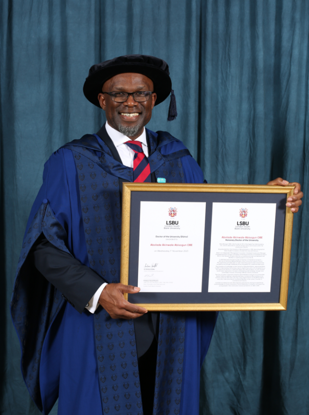
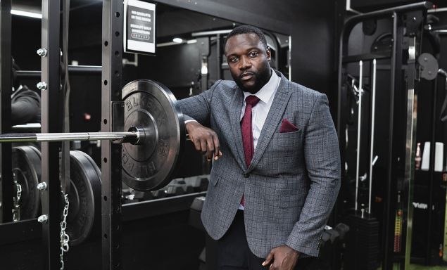
Abolade Akinwale Abisogun OBE
Carrie Rutherford, Principal of LSBU Business…
Carrie Rutherford is the Principal of LSBU Business School at our Croydon Campus.
Norman Ackroyd CBE, Honorary Doctor of the Un…

Institute of Refrigeration: a Knowledge Trans…
A priority for the Institute of Refrigeration (IOR) is the growing sensitivity regarding the environmental impact of medium and large-scale refrigerat...

Brian Blake, Honorary Doctor of the Universit…

Honorary Graduate Dame Carol Black discusses…
Dame Carol Black is an Honorary Doctor of Health and Social Care at LSBU
Janet Fyle, Honorary Doctor of the University
Rachel Gadsden talks openly about disability
Acclaimed artist Rachel Gadsden is an Honorary Doctor of LSBU. Her work explores universal themes of fragility, survival and hope, drawing on her own ...
Knowledge Transfer Partnership: increasing re…
The Daycare Trust decided to undertake a Knowledge Transfer Partnership (KTP) to improve their ability to generate new income through research and con...
Dela Idowu, Honorary Doctor of the University…
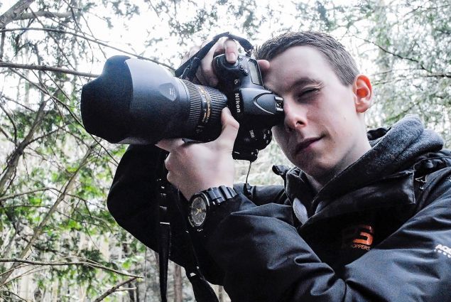
Oliver Spier, Photography Technician
Olivier Spier, a photography technician and TSS team member, discusses his role at LSBU and the new working group he's setting up for arts technicians...
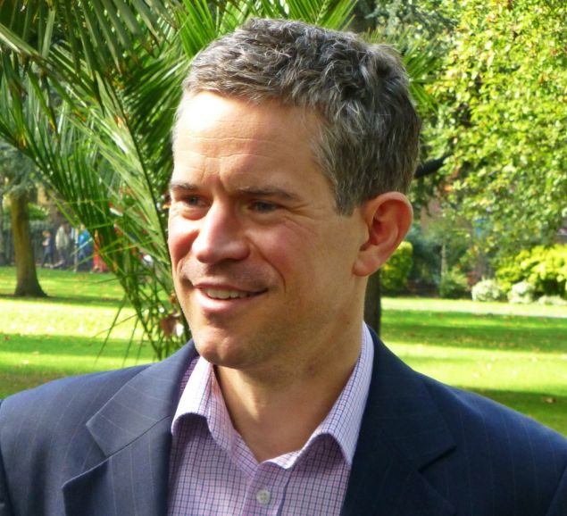
Dr Mark Williamson, honorary doctor of letter…
Dr Mark Williamson has been made an Honorary Doctor of Letters.
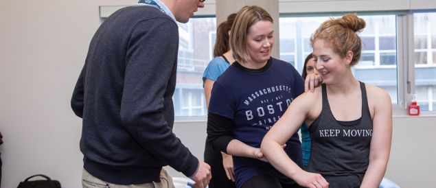
LSBU Chiropractic Clinic
The Croydon Chiropractic Clinic is run by our experienced fourth year students with the aim of providing therapy for fellow students, academics and th...